
Engineering resource · Electrical insulation
What Are Electrical Insulation Components? PCB-to-Chassis Barriers Explained
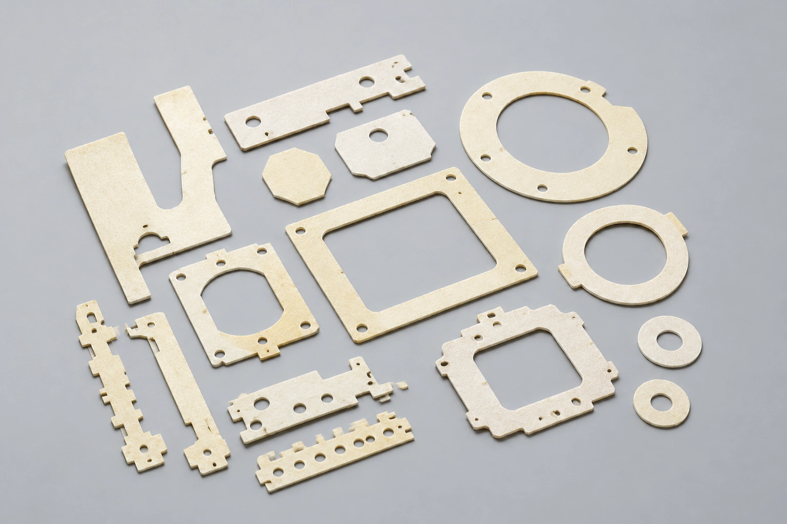
Electrical insulation components are physical parts that keep specified conductors electrically separated. Inside an electronic enclosure, a die-cut sheet can separate a circuit board from the chassis floor, a folded barrier can separate an exposed lead from a sidewall, and an insulating bushing can line a hole around a metal fastener. A roll of insulating stock becomes a useful component once its shape, openings and mounting features put the material between the right surfaces. [1, 2, 4]
A board can need insulation under a connector and deliberate metal contact at the mounting point beside it. Those two requirements belong on the same drawing. Start by finding the conductive surfaces that come closest together, then mark the ones the circuit or installation instructions require to be connected. This gives the engineer a basis for choosing a shape and the buyer a way to tell whether two proposed parts do the same job.
Where could the board touch the enclosure?
Consider a drawing review for a hypothetical printed circuit board (PCB) on metal standoffs. A through-hole connector leaves a pin projecting below the board. A bare lead at the board edge points toward the sidewall. In the bottom section view, the distance that matters starts at the end of the pin. A dimension from the board laminate to the floor overstates the free space by the length of pin below the laminate. The same mistake in a top view would be to measure from the board outline and overlook the lead extending beyond it. Cadence identifies both protruding leads and exposed solder as points to inspect. [1]
Check the views in pairs
In plan view, mark the outline of the exposed metal and the nearest sheet edge or cutout. In section, check whether the sheet actually lies between that metal and the chassis. A view from above can show the pin inside the outline of a flat sheet even though a sideways-facing lead has a clear path to the wall. Conversely, a point with no film between it and the wall does not by itself establish a fault. If the installed spacing meets the equipment requirements across the permitted positions, there may be no reason to add a barrier there.
If the longest permitted pin reaches the enclosure floor, make room first. Review the pin projection, support height or board position before adding sheet stock. A thicker sheet takes up more of the space the two parts are already competing for.
What does a flat sheet cover, and when would a folded edge help?
A flat sheet can block direct contact between the pin and the enclosure floor if it stays intact and extends beneath the pin in every allowed position. Its edge is as important as its thickness. With the sheet located by the enclosure and the board located by the standoffs, a centered prototype can hide a loss of coverage. Move the board toward the sheet edge on the drawing, then move the sheet as far as its own locating features permit in the opposite direction.
A quick way to read the result is to compare the nominal overlap with the greatest permitted relative movement toward that edge. Measure overlap from the outermost exposed metal to the boundary of intact material, including the edge of a nearby cutout. If the permitted movement uses up the overlap, the pin can reach the boundary. Extend the outline or change how the part is located. Overlap remaining on the drawing establishes coverage in that direction only. It supplies no electrical spacing or voltage rating.
Table 1. Choosing the part by the surfaces it can separate
| Candidate | Interface it can cover | What could still be exposed |
|---|---|---|
| Flat insulating sheet | Underside pin or solder joint facing the chassis floor | The lead can pass the sheet edge or lie over an opening. |
| Folded sheet barrier | Bottom face and a bare lead facing a sidewall | A short, low or unrestrained fold can leave the side lead exposed. |
| Flat insulating washer | Screw head facing a top-side copper pad | The shank, hole wall and underside copper lie outside that face. |
| Insulating bushing | Fastener shank facing a conductive bore | Only the length actually sleeved is covered. Inspect both ends and bearing faces. |
Swipe horizontally to view all columns.
For a sidewall lead, show the fold direction on the flat pattern and the finished height in section. Its length along the wall must cover the lead throughout the board’s permitted travel. The ITW Formex guide distinguishes a partial-depth cut, a crease and a perforated score. It also shows tabs that hold a part during installation and a housing that can retain it afterward. A part that holds its shape in the operator’s hand may sit differently when the cover closes. Where electrical separation depends on the fold itself, the actual score construction belongs in the assessment. The guide shows both partial-depth and full-depth perforations. A through-slit at the closest point to the lead deserves its own check. [2]
Should the barrier cover the mounting hole?
Look up the electrical purpose of that particular mounting point before drawing the cutout. A clearance hole for a screw can be wide enough for assembly while the surrounding sheet still covers the metal face that needs to make contact. Conversely, opening up more sheet around a point intended to be isolated can expose underside copper to a metal standoff.
A documented example of a connection to preserve
For the Class I installation shown on page 12 of the TDK-Lambda CUS30M manual, the power supply’s protective earth (PE) terminal must connect to the equipment’s protective earth. The same installation also calls for a metal spacer connecting mounting hole B to an earthed metal plane or chassis for electromagnetic compatibility (EMC). The drawing should therefore identify the contact footprint between the board and the spacer. A cutout that clears the screw but leaves film over that footprint could interrupt the specified connection. Apply this example to the illustrated mounting arrangement. For another board, check its own mounting instructions. [3]
Table 2. Following one fastener through a board intended to be isolated
| Location in section | Possible metal contact | What to inspect |
|---|---|---|
| Under the screw head | Head against an exposed top pad | The insulating washer must still cover the bearing area after alignment. |
| Inside the hole | Shank against a conductive hole wall | Check the wall finish, available fit and any portion of the bore left uncovered. |
| Under the PCB | Bottom copper ring against the metal standoff | Trace the standoff footprint against bare copper in the allowed positions. |
Swipe horizontally to view all columns.
The table describes the hypothetical isolated mounting point. A flat insulating washer can address the first row while the other two contacts remain possible. Figure 12 of onsemi application note AN1040/D makes the distinction visible on a different assembly, a nonisolated stud-mounted power semiconductor. A face insulator lies against the mounting surface and an insulating bushing enters the chassis hole. The figure explains why face and bore need separate attention. The choice of PCB hardware still depends on the actual hole, copper and clamping arrangement. [4]
If the electrical drawing does not identify the intent, leave a question against that mounting point for the electrical designer. The appearance of a plated hole gives procurement no basis for deciding whether to add a washer or enlarge the cutout.
What should the drawing show before you order a prototype?
Provide the flat pattern together with a section through the installed board, barrier and enclosure. Reference the cutouts, sheet edges and fold line to features that locate the actual parts. Show the exposed conductors, the limits of relative movement, the installed fold, and the metal contact faces that must stay clear. If board and sheet use different datums, show how those datums relate in the assembly. Two accurately cut parts can still be misaligned when each is measured from a different origin.
Table 3. What to record in the prototype review
| Feature | Evidence to capture | What the finding changes |
|---|---|---|
| Sheet edge under the pin | Plan view at the adverse allowed board and sheet positions | If the pin can pass the edge, revise the outline or location. |
| Fold beside the lead | Section with the cover fitted. Record fold height, direction and retention. | If the fold moves clear of the lead, change the fold or its restraint. |
| Required chassis contact | Cutout and metal bearing footprint on the same view | If film covers the footprint, revise the opening and recheck nearby copper. |
| Point identified for isolation | Section through head, shank, hole and standoff | If an unintended metal pair can meet, identify that pair before changing hardware. |
Swipe horizontally to view all columns.
An unpowered fit check answers whether the observed sample can be located, folded and retained as drawn. Record the board revision, barrier revision and the position actually checked. If the sample was centered, record that fact rather than marking the full movement range accepted. A photograph taken before fitting the cover is useful for orientation. It cannot show what holds a hidden fold after closure. Choose a view or inspection arrangement that lets the reviewer verify the feature in its assembled position.
An example note for the drawing
For the hypothetical assembly, a useful note would read, “Maintain sheet coverage beneath the projecting connector pin throughout the board movement shown in the assembly view. Keep the identified spacer contact face exposed. Verify the side fold with the cover fitted.” Fill in the project’s dimensions and identify the mounting point on the drawing. With that information a supplier can review the outline and fold, and quality staff can inspect the same features the designer intended.
How to read a material figure before putting it on a specification
Suppose a proposed prototype uses Formex GK-10. The ITW data sheet gives a nominal thickness of 0.010 in. and a typical dielectric breakdown voltage of 16,264 V. It lists ASTM D149 and IEC 60243-1 without identifying an edition. The breakdown figure belongs to the tested stock. It cannot establish a continuous working voltage for the folded component or the equipment. The adjacent rows in the same column answer different questions. [5]
Table 4. Three entries from the Formex GK-10 data sheet [5]
| Data-sheet entry | GK-10 value | How to use it |
|---|---|---|
| Nominal stock thickness | 0.010 in. nominal | Listed tolerance is +0.003 / −0.0015 in. The thick end of the range matters where space is tight. |
| Typical dielectric breakdown voltage | 16,264 V | Voltage at breakdown under the material test conditions. It is not a production minimum. |
| Typical dielectric strength | 1,626 V/mil | A thickness-normalized test value. One mil is 0.001 in. It is not an allowable design field for the assembly. |
Swipe horizontally to view all columns.
For a fit calculation, the thickest stock permitted by the listed tolerance is 0.013 in. before forming. An enclosure that leaves room for only the nominal 0.010 in. may therefore have a mechanical interference even when the supplied stock is within specification. That calculation answers whether the sheet will fit. Electrical acceptance requires different evidence. [5]
ASTM D149-25, section 5.3, explains why a material result by itself is usually insufficient to predict dielectric behavior in the finished equipment. Section 5.5 identifies variables including specimen conditioning, electrodes and how the voltage was applied. The ITW sheet is dated 2018, so the later ASTM edition helps interpret the method without establishing which edition ITW used. If a proposal relies on the number to qualify a formed fold or a different grade, ask what evidence covers that construction and intended use. [5, 6]
An opening can leave a route through air around the sheet edge, and the surface can provide a route between conductors. Clearance is the shortest separation through air. Creepage distance is the shortest path along an insulating surface. The path through the sheet depends on the solid insulation. IEC 60664-1 covers these aspects of insulation coordination for equipment in its scope in low-voltage supply systems. The product’s applicable requirements, working voltage and environment determine the electrical acceptance criteria. [7, 8]
The prototype request is ready for a useful review when the fabricator can locate the barrier, the assembler can tell which contact face to leave exposed, and the electrical designer can identify the paths that still need equipment-level verification.
Sources and technical references
The PCB drawing review is a worked example. The named equipment and material examples are documented in the manufacturer sources below. Standard references point to the publishers’ public scope or excerpts.
[1] Cadence PCB Solutions · Materials to Insulate a PCB in a Metal Enclosure
January 5, 2024. See “What Do We Need to Insulate?” for the exposed features to locate.
“Scores” and “Joinery Examples.” Cut, creased and perforated folds, plus retention during and after installation.
[3] TDK-Lambda · CUS30M Series Instruction Manual
Document CA851-04-01D, pp. 11–12, especially p. 12, item (3). The illustrated Class I installation.
[4] onsemi · Mounting Considerations for Power Semiconductors
AN1040/D, Rev. 5, August 2021, p. 10, Figure 12. Face insulators and a bore bushing.
[5] ITW Formex · Formex GK Product Data
February 22, 2018, p. 1. Read the GK-10 column, the thickness tolerance and both typical electrical-property rows together.
[6] ASTM International · ASTM D149-25
Public “Significance and Use,” sections 5.3 and 5.5. Interpretation of results and test variables.
[7] IEC · IEC 60664-1:2020+AMD1:2025 CSV
Edition 3.1. Published scope for low-voltage insulation coordination.
[8] Weidmüller · Clearance and creepage distances
Published definitions of the shortest air and surface paths between conductors.